
How Flex PCB Manufacturing Handles Tight Tolerances
Flex PCB Manufacturing
Flex PCBs are used in a wide range of electronic devices, especially mobile phones, tablets, and handheld electronics. Because they combine rigid support structures with flexible circuitry, flex circuits are ideal for devices that require durability and reliability in small package sizes.
While the flexibility of flex PCBs makes them ideal for small and tight spaces, the materials they use must be durable enough to withstand mechanical stress. This is why it is important to work closely with your flex manufacturer early in the design phase to ensure that your flex circuit board is manufacturable and will meet your requirements.
A face-to-face meeting with a flex supplier will help you ensure that your manufacturing process is on track, and that you’re both on the same page regarding what can be achieved with a given layout. This will reduce the number of errors that may occur during production and assembly, and can result in a more accurate and reliable flex circuit board.
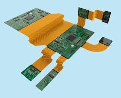
How Flex PCB Manufacturing Handles Tight Tolerances
The most common flex pcb manufacturing are rigid-flex boards. These are fabricated with rigid copper layers on top of an adhesive-based or adhesiveless polyimide layer. The copper is either bonded with acrylic adhesive or cast directly onto the polyimide using a specialized casting technique. Rigid-flex circuits are also available with metallized surface finishes that improve electrical performance and resistance to corrosion.
For a flex PCB to perform well, it must be able to withstand high-speed signals without losing signal integrity. To ensure this, designers use simulation tools to test the behavior of signals. These tools allow them to simulate real-world conditions and highlight potential areas of concern, such as reflections and jitter. This allows designers to iteratively refine their flex PCB designs to address these issues before moving to physical prototypes.
Identify the flex and rigid regions of your flex PCB during the layout phase. Then, calculate the minimum bend radius for each region to determine how much force is required to damage the circuit. Avoid overlapping rigid and flex regions and place vias in stress-free zones to prevent cracking. Incorporate S curves in trace routing to improve flexibility and reduce stress. Opt for hatched ground planes instead of solid ones, as they have higher flexibility.
The thickness of the flex PCB stack-up impacts its ability to flex, as well as its ability to resist thermal cycling. Choose a thin material like polyimide or polyester (PET) for standard circuits, and a high-temperature resistant material such as polyimide or epoxy for high-frequency applications. Choosing a flexible material with low moisture absorption can also improve performance and reliability.
The flex PCB fabrication and assembly processes must be carefully planned to ensure that components are properly aligned with the underlying copper layer. This will prevent solder joints from bending and warping during assembly, which can cause failures. Stiffeners can be added to a flex PCB to improve its mechanical rigidity, especially around mounting points. It’s also a good idea to avoid putting components directly on the flex substrate. Doing so could lead to solder joint failures due to dimensional variation.